
Achieving an average assembly yield of 99.74 percent across millions of sites suggests that liquid-based integration is becoming a viable path for mass-producing AR hardware. This achievement addresses the notorious screen door effect that has plagued immersive headsets since their inception, where visible gaps between pixels break the suspension of disbelief for users. To eliminate these visual artifacts, display engineers are pushing beyond the conventional limits of mobile screen technology, which typically maxes out at around 460 pixels per inch. The target for modern augmented reality is now 2000 PPI or higher, a requirement that places immense strain on traditional manufacturing pipelines. Inorganic nano-LEDs have emerged as the primary solution for these high-density demands due to their superior brightness and durability compared to organic alternatives. However, the true difficulty lies in the massive scale of assembly, requiring the precise placement of millions of microscopic light sources onto a single substrate without errors.
Mastering Alignment: Dielectrophoresis and Microwells
To solve the spatial arrangement of these microscopic components, the industry has turned toward dielectrophoresis as a primary alignment tool. By utilizing alternating electric fields within a specialized fluid medium, manufacturers can exert precise control over gallium nitride nano-rods as they move toward the display substrate. This technique leverages the polarization of the particles, forcing the long axes of the nano-LEDs to align with the orientation of the field. Unlike previous fluidic assembly attempts that suffered from chaotic particle movement and random rotations, dielectrophoresis provides a reliable force that guides each rod into its designated orientation. This controlled movement is essential because even a slight angular misalignment can prevent proper electrical contact or lead to uneven light distribution. The implementation of this electrical guidance system marks a shift from passive deposition to active, deterministic assembly, enabling the high-speed processing of millions of emitters simultaneously.
Complementing the electrical guidance is the use of precision-engineered microwells etched into the substrate, which act as physical traps for the incoming nano-LEDs. These wells are designed with specific dimensions that allow for the entry of exactly one rod, effectively preventing the clumping or overcrowding that often ruins high-density displays. When a nano-LED enters a microwell, it alters the local electric field in a manner that repels subsequent particles, creating a self-limiting mechanism that ensures a perfect one-to-one ratio between emitters and pixel sites. This spatial precision is a critical step in avoiding crowded pixels that could lead to thermal hotspots or electrical shorts. By combining the physical constraints of the wells with the dynamic forces of dielectrophoresis, the system achieves a level of uniformity that was previously impossible. This dual-layer approach effectively bridges the gap between nanoscale physics and macroscale manufacturing, providing a scalable solution for complex AR systems.
Validating Performance: Precision and Scalability
The statistical validation of this assembly method reveals a significant leap forward for the semiconductor industry, with recorded yields reaching 99.74 percent across large-scale arrays. Such a high success rate is mandatory for commercial applications, as a single percent of failure would result in thousands of dead pixels, rendering a high-resolution display unusable for the consumer market. These results demonstrate that liquid-based assembly is no longer confined to small laboratory experiments but is capable of producing centimeter-scale display panels with industrial-grade reliability. The consistency of this process across millions of sites suggests that the hardware for high-fidelity wearable technology can finally move into mass production. Moreover, the ability to maintain these yields while increasing the density of the emitters suggests that the technology is robust enough to handle the next generation of visual requirements. This progress indicates that the assembly bottleneck is finally being dismantled by innovative fluidic techniques.
Precision at the sub-micron level is another cornerstone of this manufacturing breakthrough, with researchers reporting an average placement offset of only 0.06 micrometers. This level of accuracy is vital for the subsequent stages of device integration, particularly when establishing electrical connections between the nano-LEDs and the underlying circuitry. In a display where pixels are spaced only a few micrometers apart, a minor misalignment could cause a total failure of the electrical grid or lead to cross-talk between adjacent color channels. By ensuring that each light source is centered almost perfectly over its corresponding electrode, the assembly process facilitates a stable and low-resistance contact for the conductive layers. This microscopic alignment also simplifies the deposition of top-side contacts, as the predictable position of the emitters allows for the use of standard photolithography and metallization techniques. The reduction in placement error directly translates to higher device performance and a more streamlined manufacturing workflow.
Prototyping Success: High-Resolution Display Metrics
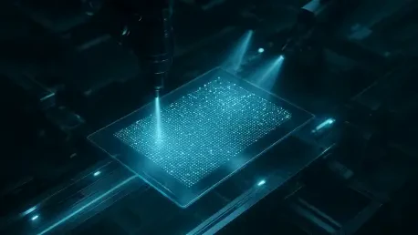
The practical application of these techniques has culminated in a functional prototype that showcases the future of near-eye display technology. This blue light-emitting panel achieves a pixel density of 2936 PPI, packing nearly one million individual nano-LEDs into a compact area suitable for integration into AR glasses. The device demonstrates stable optical performance and remarkably low leakage current, proving that the liquid-based assembly process does not compromise the electrical integrity of the inorganic materials. This prototype serves as a proof of concept for the feasibility of using billions of nano-rods to create seamless digital environments. The high brightness levels inherent to inorganic gallium nitride ensure that the display remains visible even in bright outdoor environments, a feat that current organic light-emitting diodes often struggle to achieve. By successfully operating at such high densities, the prototype confirms that the assembly bottleneck can be bypassed without sacrificing the quality or longevity of the display hardware.
Looking toward the broader market, the next challenge involved the integration of full-color RGB capabilities into these high-density arrays. Current research is exploring several paths, including the use of quantum dot color-conversion layers or the simultaneous assembly of red, green, and blue nano-LEDs. Successfully managing multiple colors within the same fluidic process will require further refinement of the dielectrophoretic sorting mechanisms to ensure each color rod lands in its designated zone. Additionally, the transition to consumer-ready hardware will involve the direct integration of these nano-LED arrays onto silicon backplanes, which provide the high-speed switching and power management necessary for fluid visual experiences. This synergy between advanced nano-assembly and traditional silicon manufacturing is expected to drive down costs while increasing the performance of head-mounted displays. As these technologies mature, they will enable the creation of sleek, lightweight glasses that provide a level of visual fidelity indistinguishable from the physical world.
Strategic Integration: Future Manufacturing Standards
The path toward solving the assembly bottleneck was paved by years of experimentation with fluid dynamics and electrostatics at the nanoscale. Researchers previously struggled with the random behavior of particles in solution, which often led to low yields and non-functional displays that hindered the growth of the augmented reality sector. However, the introduction of dielectrophoretic control and precision-engineered microwells changed the landscape of the industry. This technological shift allowed manufacturers to move away from the slow and expensive methods used in the early stages of display development. By proving that millions of components could be organized with sub-micron precision, the industry established a new foundation for high-density light-emitting arrays. These early breakthroughs were essential in demonstrating that the visual requirements for immersive digital environments could be met using inorganic materials. The successful creation of high-PPI prototypes validated the theoretical models and provided the necessary evidence to attract significant investment.
Moving forward, the focus shifted toward standardizing the fluidic assembly process across the semiconductor industry to foster a competitive ecosystem of display components. Developers prioritized the creation of modular assembly platforms that were adapted to different types of nano-emitters, including future micro-laser diodes and alternative light-source architectures. Furthermore, the integration of real-time optical inspection systems into the assembly line allowed for the immediate identification and correction of minor defects, further pushing the boundaries of manufacturing yield. Collaborative efforts between material scientists and software engineers optimized the drive electronics for these ultra-high-resolution displays, ensuring that the processing power of the headsets kept pace with the massive amount of visual data. As these manufacturing hurdles were cleared, the industry expanded the application of nano-LED arrays into other fields such as holographic projection and advanced medical imaging, where extreme resolution and brightness were equally transformative.