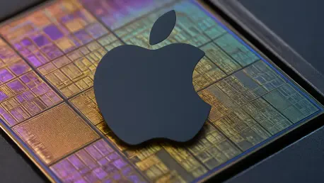

The silicon landscape is witnessing a seismic shift as the limits of physical miniaturization once thought insurmountable are being methodically dismantled by the engineering alliance of Apple and TSMC. As 2026 unfolds, the industry is no longer merely speculating about the feasibility of sub-nanometer chips but is instead actively preparing for a transition that will redefine the computational capabilities of every device in the consumer ecosystem. This partnership has historically allowed Apple to dictate the pace of hardware innovation, and the current move toward 1.4nm and 1nm architectures suggests a strategy designed to maintain that dominance for the next half-decade. By securing exclusive access to the most advanced fabrication nodes, the company is effectively insulating its product lineup from the diminishing returns of traditional silicon. This trajectory ensures that the iPhone, iPad, and Mac platforms will continue to offer performance-to-power ratios that remain out of reach for competitors.
The Road to the Sub-Nanometer Era
Strategic Milestones: The Path to A10 Fabrication
The transition toward 1nm architecture involves a series of calculated steps, moving from current 3nm standards and upcoming 2nm production to the trial of the “A10” process by 2029. To maintain a competitive edge, Apple is expected to strategically skip certain iterations, such as the 1.6nm node, to focus its vast resources on the 1.4nm and 1nm thresholds. This aggressive roadmap suggests that by 2030, consumers will have access to hardware powered by processors that are significantly more advanced than anything currently available on the market. The decision to bypass intermediate steps reflects a high-stakes gamble on long-term technological superiority over short-term incremental updates. By consolidating research efforts into these “leapfrog” nodes, Apple can ensure that its silicon remains several generations ahead of the broader industry. This approach also allows for a more streamlined development cycle for its internal engineering teams.
Securing the primary capacity of TSMC’s upcoming fabrication facilities provides Apple with a unique defensive moat against other tech giants who are also vying for limited foundry space. As the demand for high-performance silicon continues to outpace supply, being the first in line for 1.4nm technology in 2028 creates a hardware bottleneck for competitors who must wait for later production cycles. This exclusivity is not just about raw speed; it is about the ability to offer features that are physically impossible on older, less efficient nodes. For instance, the increased transistor density of 1nm chips will likely enable sophisticated on-device machine learning models to run with negligible impact on battery life. The strategic alignment between the chip designer and the manufacturer serves as a blueprint for the next decade of mobile computing, ensuring that the flagship devices of 2030 will possess capabilities that were once reserved for high-end server racks.
Material Science: Beyond Traditional Silicon
Reaching the 1nm milestone requires moving beyond traditional silicon toward innovative materials like bismuth to overcome the physical limitations of electron leakage and thermal management. These technical shifts, combined with Apple’s deep vertical integration, are projected to yield a thirty percent boost in overall performance and power efficiency compared to current chip generations. Such gains allow Apple to maximize performance per watt, which is essential for maintaining high profit margins and ensuring that devices can handle intensive tasks without requiring excessive memory or battery capacity. The transition to bismuth-based semiconductors marks one of the most significant changes in chip manufacturing since the introduction of FinFET transistors. It addresses the fundamental issue of resistance at the atomic scale, allowing electrons to move more freely through increasingly narrow channels without generating destructive levels of heat.
Furthermore, the integration of these new materials allows Apple to rethink the entire internal architecture of its devices, from the way heat is dissipated to the physical layout of the logic board. By reducing the thermal footprint of the processor, engineers can allocate more space to other components or reduce the overall thickness of the chassis. This material evolution is also a hedge against the rising costs of traditional semiconductor components. As the price of high-capacity RAM continues to fluctuate, the efficiency of 1nm chips allows Apple to achieve superior user experiences with less physical memory than its rivals. This “efficiency first” philosophy ensures that the company can protect its bottom line while still delivering a product that feels faster and more responsive to the end user. The shift toward bismuth is therefore both a scientific necessity and a shrewd economic strategy for the coming decade.
Navigating Global Market Shifts
Stability Amidst the Artificial Intelligence Boom
While the tech industry is currently fixated on massive investments in AI server chips, Apple remains the most reliable anchor for TSMC’s long-term business model. As the potential bubble for server-side AI fluctuates due to soaring energy costs and infrastructure challenges, Apple’s consistent demand for high-volume consumer hardware provides the financial foundation TSMC needs to justify multi-billion dollar research costs. This symbiotic relationship ensures that even as the market shifts toward “edge AI”—where data is processed locally on the device rather than in a cloud center—Apple will have the superior silicon necessary to lead that transition. The stability of the consumer electronics market acts as a counterweight to the volatility of the enterprise sector, allowing for steady progress in fabrication technology. This ensures that the development of 1nm nodes continues unabated by market trends.
The shift toward local processing is particularly important as privacy concerns and latency issues drive more users away from cloud-dependent services. By having the most powerful and efficient chips on the market, Apple can offer a level of privacy that competitors using less advanced silicon simply cannot match. Processing complex AI tasks on a 1.4nm or 1nm chip requires significantly less energy, making it feasible to run “always-on” intelligence features without draining the battery of a smartphone or wearable. This focus on edge computing aligns perfectly with the current industry move toward decentralized data handling. As the initial frenzy over massive AI data centers begins to stabilize, the focus will inevitably return to the devices people carry in their pockets. Apple’s early investment in sub-nanometer technology positions it to capture this shift, turning its hardware into the primary gateway for personalized artificial intelligence.
Revolutionary Form Factors: The Future of Wearables
The dramatic reduction in heat generation and power consumption afforded by 1nm chips will fundamentally change how Apple products look and feel in the future. These advancements will likely lead to the creation of ultra-thin “MacBook Neo” designs and powerful augmented reality glasses that pack the performance of a modern computer into a lightweight frame. By shrinking the internal components, designers can prioritize sleek aesthetics and portability without compromising the raw power users expect from the ecosystem. This technological leap is particularly critical for the development of wearable devices that must remain comfortable for all-day use. Current limitations in battery density and thermal dissipation have often forced a trade-off between performance and wearability, but the 1nm era aims to eliminate those compromises entirely. This will allow for a new class of “ambient” devices that blend seamlessly into daily life.
Beyond laptops and tablets, the move to 1nm silicon opens the door for a resurgence in specialized hardware that was previously deemed impractical. For example, high-fidelity audio processing and advanced health monitoring sensors can be integrated more deeply into the silicon, providing real-time data analysis without taxing the device’s main processor. This level of integration is only possible when the power budget of the chip is measured in milliwatts rather than watts. As Apple continues to push the boundaries of what its silicon can do, the very definition of a “computer” will continue to evolve. The future of the brand may not be defined by a single flagship device, but by an interconnected web of highly efficient, specialized hardware that works in concert. The 1nm node is the key that unlocks this vision, providing the necessary density to fit desktop-class power into the smallest possible enclosures while maintaining a cool and quiet user experience.
Supply Chain Security: Safeguarding Against Geopolitics
The path to 1nm technology is not without significant external risks, particularly regarding the geopolitical tensions between the United States and China. To mitigate these threats, TSMC is expanding its fabrication capacity within the United States, a move that serves as a vital insurance policy for Apple’s supply chain. This diversification of manufacturing helps protect the production of next-generation chips from regional instability, ensuring that Apple’s technological evolution remains on track regardless of international diplomatic shifts. By moving critical production closer to its primary markets, the company reduces the risk of long-term shipping delays and export restrictions. This geographic shift is a massive undertaking that requires years of coordination and billions in capital, but it is a necessary step to ensure that the transition to 1.4nm and 1nm chips remains uninterrupted by global politics.
The construction of state-of-the-art foundries in locations like Arizona represents a turning point in the semiconductor industry. For Apple, this means that the journey toward the sub-nanometer threshold is supported by a more resilient and geographically diverse infrastructure. This strategy not only secures the hardware roadmap but also provides a level of certainty to investors and consumers alike. As the world becomes increasingly reliant on advanced silicon, the stability of the supply chain becomes as important as the technology itself. By supporting TSMC’s expansion and securing early production slots in these domestic facilities, Apple has effectively insulated its future product launches from the unpredictability of international relations. This multi-layered approach to manufacturing ensures that the next five to seven years of innovation will proceed according to plan, regardless of how the global landscape may shift in the coming decade.
Final Outlook: A Unified Technological Vision
The strategic roadmap for Apple Silicon evolved into a comprehensive plan that prioritized long-term stability and material innovation over immediate, incremental gains. By 2026, the company successfully bridged the gap between current standards and the upcoming 1nm frontier, ensuring that its hardware remained the benchmark for efficiency. The collaboration with TSMC allowed for the exploration of new materials like bismuth, which addressed the looming physical constraints of traditional silicon. This foresight enabled the development of thinner, more powerful devices that integrated seamlessly into the lives of users. Furthermore, the expansion of manufacturing facilities provided a necessary buffer against the geopolitical uncertainties that threatened the global supply chain. Ultimately, the push for sub-nanometer chips secured a future where computational power was no longer limited by heat or size, paving the way for a new generation of ambient and wearable technology.